Atomically Thin Gallium Layers Gallenene
2D materials research began with the isolation of graphene, but it has expanded to include many other materials, all in an effort to develop new nanoplatforms for research and industrial applications that can outperform graphene.
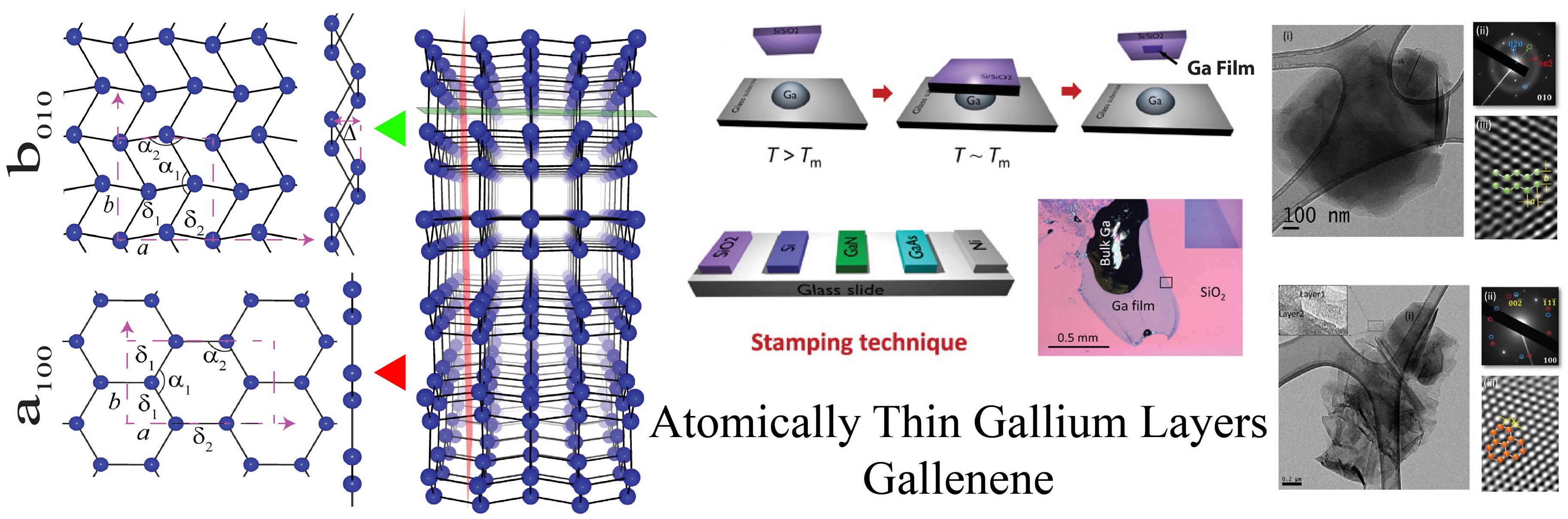
“Gallenene”: Theoretically predicted two distinct atomic arrangements of monolayer of Ga oriented along two crystallographic (010) and (100) directions, respectively. The corresponding layers in bulk gallium are also shown. A simple exfoliation technique of surface solid layers from the molten phase of Ga to synthesize these 2D metallic sheets are also shown. The shown TEM images and the theoretically predicted structures are in excellent agreement.
Gallium, with its rich low-temperature phase diagram, is a liquid metal at room temperature and displays impressive potential for use as a 2D material. The conventional deposition technique for Ga does not provide freedom to select the substrate, which is one of the major requirements for using atomically thin Ga for multiple applications. Theoretical and experimental investigation by groups of A. K. Singh at IISc and P. M. Ajayan at Rice University, USA introduce a new approach for realization of thin 2D sheets of gallium, called as “gallenene”. The density functional theory calculations demonstrate that atomically thin gallenene can be stabilized on a substrate in two distinct atomic arrangements oriented along two crystallographic (010) and (100) directions. The theoretical prediction was verified by an ingeniously simple exfoliation technique of surface solid layers from the molten phase of Ga, which yields gallenene. One-to-one correspondence between the gallenene structures as observed in TEM and the theoretically predicted structures confirmed the formation of stable 2D gallenene sheets. The exfoliation technique from solid-melt interfaces of low melting metallic materials could be a generic technique to obtain atomically thin layers of many materials.
 The gallenene strongly interacts with its substrate, which was observed in both experiments and theoretical predictions. The gallenene contacts transform the MoS2 from a semiconductor to metallic phase, resulting in better 2D contacts for devices. Dirac cone and a highly dispersive band near the Fermi level provides excellent opportunities to explore its applications as a 2D metal in plasmonics, sensors, and electrical contacts.
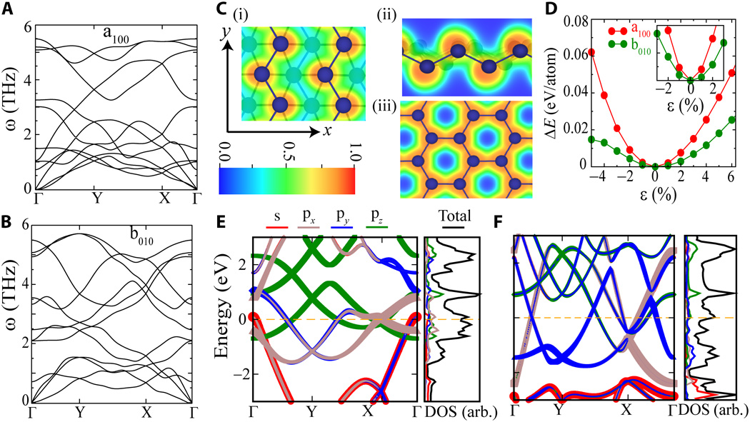
Stability and bandstructure of gallenene polymorphs. (A and B). Phonon dispersion of 6 and 2% uniformly strained monolayers of a100 and b010, respectively. (C) ELF of 2% strained structure of b010 along (i) y direction and (ii) x direction and 6% strained structures of a100 (iii) monolayers. The ELF is shown by the color bar, with red (blue) showing maxima (minima). The ELF shows uniform covalent bonding behavior in a100 gallenene and a mixture of covalent and metallic in b010 gallenene. (D) Total energy per atom with respect to the lowest-energy structure as a function of uniform strain. The inset shows ∆E for a smaller range of strain. (E and F) Orbital projected band structure, total density of states (DOS), and partial density of states of stabilized (strained) a100 and b010 monolayers with Fermi energy (EF) set to 0 eV. The electronic structure of the gallenene films is highly anisotropic with a combination of partially filled Dirac cones and nonlinear dispersive bands, which can lead to new fundamental phenomena and a wide range of applications for Ga-based 2D materials.
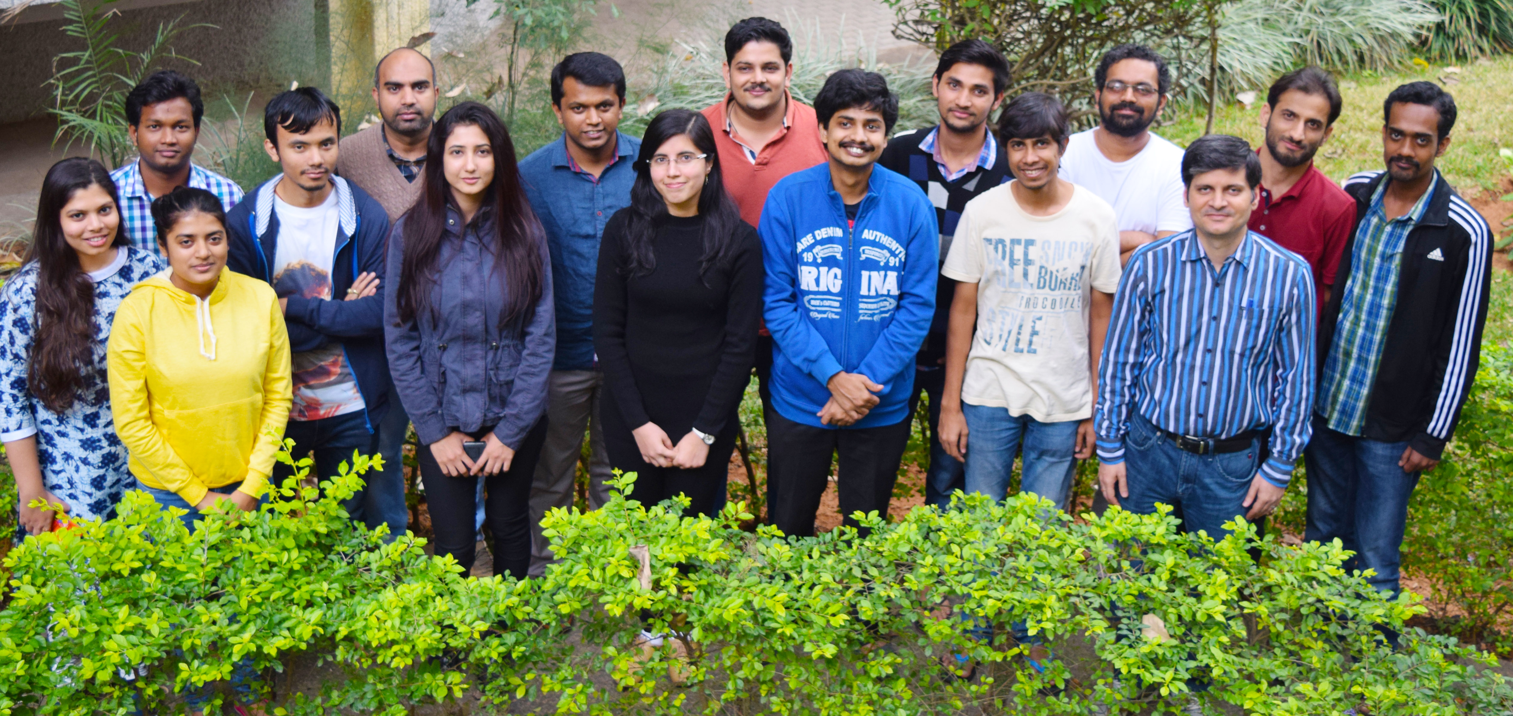
The group picture of A. K. Singh lab: in the front row (from left to right) Abhishek K. Singh and Atanu Samanta, and rest of the group members
Reference:
- Kochat*, A. Samanta*, Y. Zhang, S. Bhowmick, P. Manimunda, S. A. S. Asif, A. Stender, R. Vajtai, A. K. Singh, C. S. Tiwary, P. M. Ajayan, Atomically thin gallium layers from solid-melt exfoliation Science Advances , 4, e1701373 (2018).
Website: http://www.mrc.iisc.ac.in/abhishek-singh/