India’s first e-mode Gallium-Nitride Power Transistor
Why GaN HEMT?
All electronic devices that we use today have components made of semiconductors, mostly silicon. In recent years, gallium nitride (GaN), another semiconductor, is making its way into electronics as it is better suited for high power and high-frequency applications. Since GaN technology is still evolving, and it is less expensive to set up a foundry for manufacturing, it is touted to be India’s opportunity to mark its presence in the niche field of semiconductors. A interdisciplinary group of faculty members at IISc have developed India’s first-ever e-mode gallium nitride power transistor, whose performance is comparable to some of the best reports till date.
Power electronic systems that operate at high power and frequencies are projected to use specific transistors called High Electron Mobility Transistors or HEMTs. These transistors are made with gallium nitride, and they can operate at very high voltages, switch ON and OFF faster, and occupy less space when compared to silicon-based transistors. The projected market for HEMTs is projected to cross 5 Billion US$ and overall power device market is set to cross 18B$ mark by 2020, so one can say that GaN will acquire a major market share. With a growing market for electric vehicles in India, such an indigenous development to manufacture these transistors in India will save import costs and make us self-reliant for transistor technology.
What were the challenges with e-mode HEMT?
A High Electron Mobility Transistor (HEMT) has a conducting channel between two terminals, source and drain, and the current through the channel is controlled by a third terminal called gate. The HEMT channel is in a conducting state, or ON, unlike some of the other transistors, so current can pass through it as soon as it is powered on. To stop the flow of current, negative voltage needs to be applied at gate. However, for a transistor to operate reliably in power electronic circuits, it needs to be in the OFF state when no gate voltage is applied, which can then be turned ON by applying a voltage at the gate. Such operation is called e-mode or enhancement mode operation.
Commercially available transistors use various techniques to keep the transistor in normally OFF state One such approach is to completely recess the channel—which results in reducing the channel size. However, this affects the stability, performance and reliability of the device. Another approach is to use a gate made of gallium nitride, doped with impurities that deplete electrons from the channels and switch it OFF. The challenge with this method is that the gate and the channel form a diode, which starts conducting current when a voltage greater than a certain value is applied at the gate, making the unusable. Therefore, there was a need to build a new kind of e-mode HEMT, which is in the OFF state by default and works like any other commonly used transistor . Besides, it must be stable, reliable, efficient and can operate in the desired high voltage.
What is the New HEMT Technology Developed by IISc?
With the hardwork of two years paying off, the team at IISc were able to develop the first-ever e-mode gallium nitride power transistor from India that operates at 600V. It has many advantages in terms of performance and power handling capacity over similar devices proposed by other researchers, some of which are now in the market. Given that the 600V class e-mode HEMT technology recently got commercialised, IISc’s competition was with industry-standard state-of-the-art power gallium nitride HEMT technology. Keeping system level requirements in mind, this group has developed both e-mode HEMT as well as GaN Schottky diodes. Their work has been published in the IEEE Transactions on Electron Devices.
The researchers explored oxides of copper, nickel, aluminium and titanium for using them to make the gate of the improvised HEMT. They zeroed in on titanium oxide as it had minimal leakage current and provided better control of the voltage needed to turn the transistor ON. They finally used aluminium titanium oxide as the percentage of aluminium could be controlled during the fabrication process, which acts as a ‘control knob’, regulating the voltage needed to turn the transistor ON. Since aluminium titanium oxide is stable, it results in high reliability of the transistor.
Interestingly, the addition of aluminium in the titanium oxide was an accidental discovery! The team was experimenting with titanium oxide, trying to finetune it to achieve optimal characteristics. A particular lot that they had developed displayed characteristics totally inconsistent with, but better than, any previous lots. Investigation showed that there had been aluminium contamination, after which, the team explored the use of aluminium doping in titanium oxide.
The researchers carried out rigorous design of experiments, processed over 200 process lots to develop this technology and tested more than 150 transistors per manufacturing lot to develop the confidence with statistics. They found that the gallium nitride transistors with aluminium titanium oxide gate had a 100 fold reduction in the leakage current and better gate control, while keeping it under e-mode, as compared to other conventional GaN HEMTs. Besides, the current carrying capacity of the transistor when it is turned ON was found to be at par with industry standards.
Who Funded this Project?
This project has been funded by the Advanced Manufacturing Technology (AMT) initiative of Department of Science and Technology (DST), Govt. of India, with an initial support of 10.28 Crores. The key objective of DST’s AMT division, as far as this project is concerned, is to enable indigenous development of technologies, which are key to the nation’s economic and strategic growth. The GaN activity in IISc was seeded by the Ministry of Defence (MoD), which was subsequently supported by the Ministry of Electronics and Information Technology (MeitY) for the development of GaN based power electronics. These initiatives by MoD and MeitY on materials and devices have helped lay the platform for this advancement.
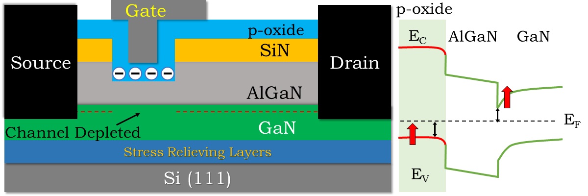
Fig. 1 Device structure depicting proposed novel p-type gate oxide for achieving normally-OFF operation in GaN HEMTs and energy band diagram depicting the proposed concept.
Reference :
- Dutta Gupta et al., “Positive Threshold Voltage Shift in AlGaN/GaN HEMTs and E-Mode Operation By AlₓTi₁₋ₓO Based Gate Stack Engineering,” in IEEE Transactions on Electron Devices. doi: 10.1109/TED.2019.2908960
Press Articles :
https://timesofindia.indiatimes.com/home/science/iisc-faculty-change-game-with-indias-first-e-mode-gallium-nitrade-power-transistor/articleshow/69661844.cms
http://www.semiconductor-today.com/news_items/2019/may/iis_100519.shtml
https://researchmatters.in/news/iisc-develops-india%E2%80%99s-first-e-mode-gallium-nitride-power-transistor


