Hierarchical structures, strain-assisted nanofabrication, and optoelectronic spectral shaping
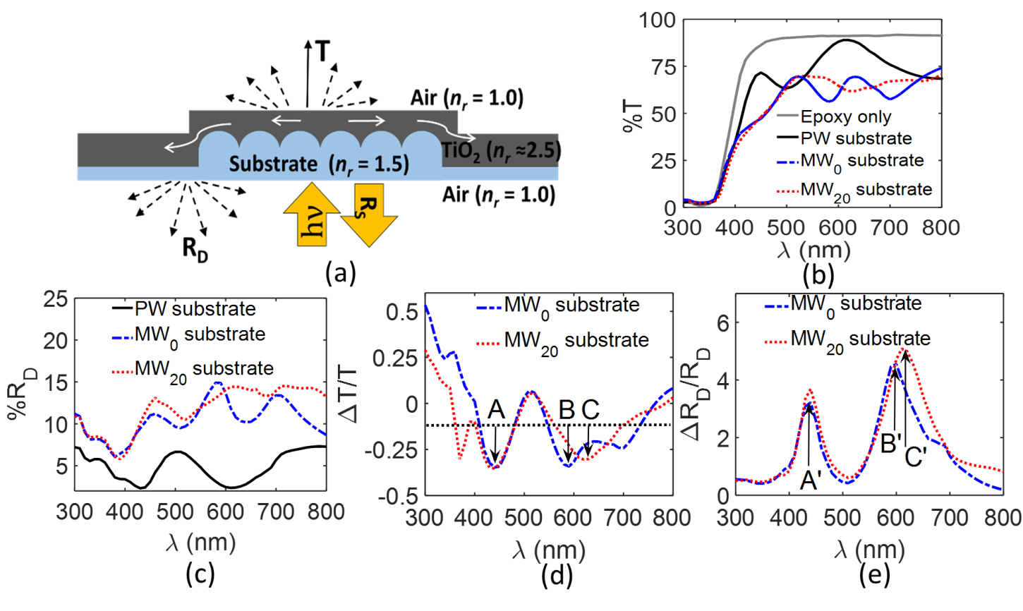
Hierarchically structured materials, comprising of structuring at multiple length scales, allow unusual modes of optical transport which are not possible in simpler structures. These processes can allow interesting ways to tailor and improve optoelectronic performances of solar cells, photodetectors etc. Here, a multidisciplinary team of researchers from Materials Engineering, BioSystems Science and Engineering, and Aerospace Engineering at IISc have demonstrated an optical confinement phenomenon in a hierarchically structured waveguide platform consisting of alternating clusters of nanostructured and planar microscale domains. Typically, defect-free nanostructured arrays are considered as the best candidates, in optoelectronic design, for light trapping. However, defective structures, such as the ones considered here, could have rich possibilities for unusual optical transport which is overlooked by conventional designs.
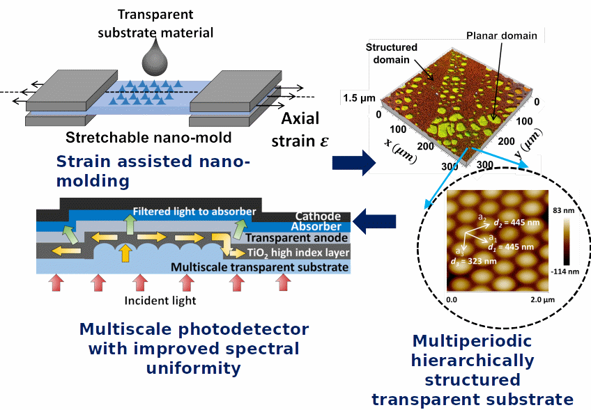
The fabrication of complex micro-nano structures would typically require a clean-room environment. However, the team developed an unconventional, strain-assisted, self-assembly-based fabrication process using commonly available moldable materials, to obtain hierarchically structured platforms. The new process facilitates the fabrication of multi-periodic nanostructures which extends the capabilities of the fabrication process beyond the state-of-the art nanofab. based processes. The team successfully fabricated waveguides on these hierarchically structured platforms and in turn used these ‘waveguide filters’ as substrates for fabricating photodetectors. The optical confinement is occurring due to the combined nanoscale scattering and the wavelength dependent interaction between the planar and structured microclusters that lead to an improved uniformity in the optoelectronic spectral response of these photodetectors. Furthermore, by tuning the multiperiodicity within the nanostructured domain structure, using a mechanical strain of 20%, an improvement of around 10% in the uniformity of the optoelectronic spectral response of the photodetectors is achieved. Simulation studies further show that these processes arise only in the presence of a hierarchical structure, and are not likely to occur in continuous or defect-free nanostructured architecture. Therefore, hierarchical structures can address optoelectronic problems that cannot be addressed by simpler structures. In summary, the experimental results supported by simulation results confirm the advantage of such unconventional approaches in design and fabrication of hierarchically structured optoelectronic platforms, and thus are expected to pave new avenues to solve optoelectronics-related engineering problems through hierarchical and multiscale structuring of materials. The proposed design and fabrication approaches can be extended, in principle, to a variety of existing optoelectronic designs and could break the performance bottlenecks posed by state-of-the-art designs.
The work has been published in the journal “Advanced Optical Materials” in June 2019. The details are available in the full-length paper.
References :
- Jagdish A Krishnaswamy, Kumar M P, Sandeep B S, Praveen Ramamurthy, Debiprosad Roy Mahapatra, and Gopalkrishna Hegde, “Shaping Resonant Light Confinement and Optoelectronic Spectra Using Strain in Hierarchical Multiscale Structures” Adv. Optical Mater.1900471, (2019) DOI: https://doi.org/10.1002/adom.201900471
- Krishnaswamy Jagdish; Kavita Garg, Ramamurthy Praveen; Roy Mahapatra D.; Hegde Gopalkrishna “Moldable biomimetic nanoscale optoelectronic platforms for simultaneous enhancement in optical absorption and charge transport” Nanoscale (RSC) (2018) DOI: http://dx.doi.org/10.1039/C7NR09015C